Tensor CoreTensor Core
Tensor Core 也是一种 GPU 核心 (core),能够通过单条指令对整个矩阵进行操作。
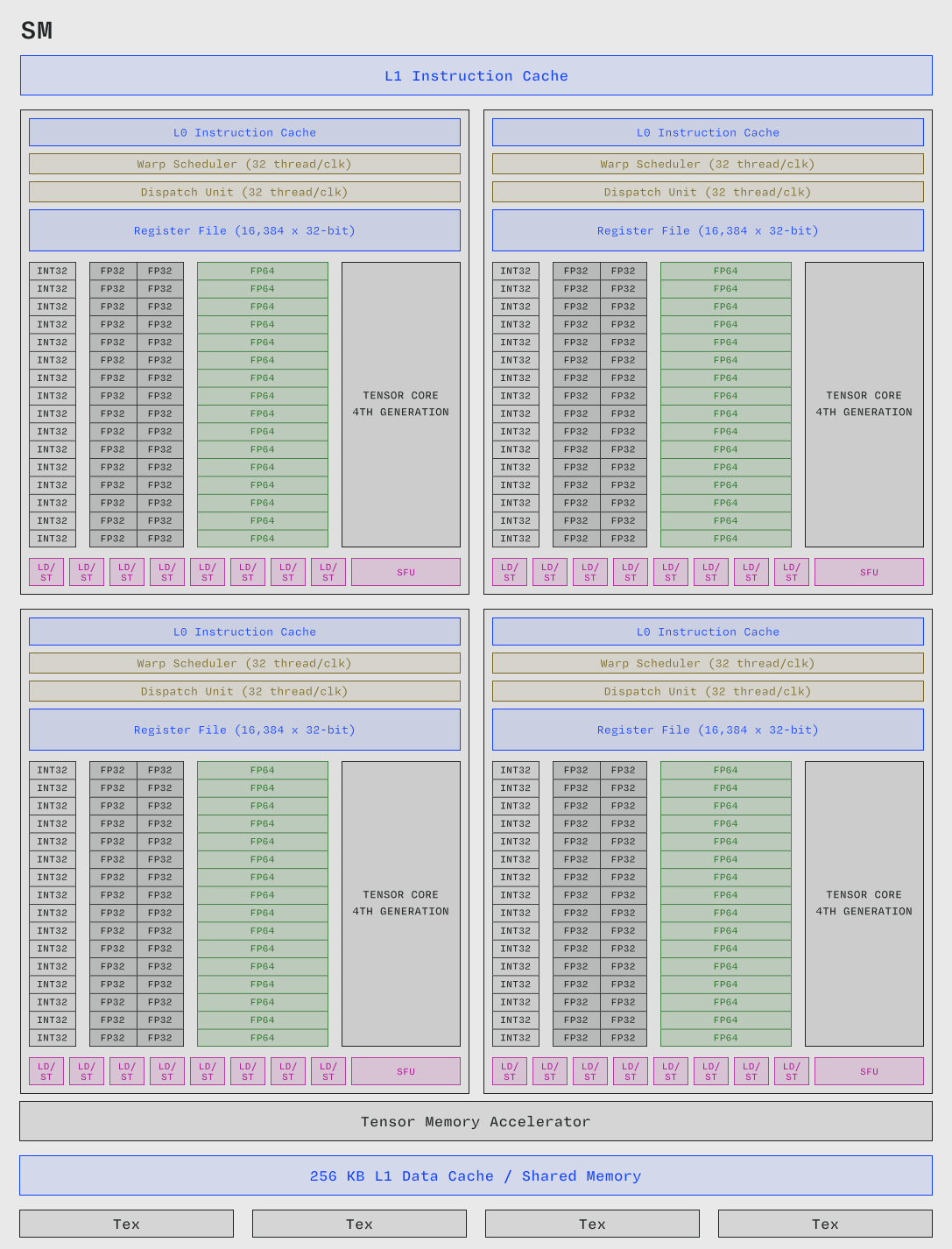
H100 流式多处理器(SM)的内部架构图。注意 Tensor Core 数量更少但尺寸更大。改编自 NVIDIA 的 H100 白皮书。
单条指令操作更多数据,可显著降低功耗需求,从而释放更高性能(参见 NVIDIA 首席科学家 Bill Dally 的 这个演讲 自 Volta 架构引入 流式多处理器 (Streaming Multiprocessor, SM) 以来,Tensor Core 已成为在 NVIDIA GPU 上实现最高 算术吞吐量 (arithmetic throughput) 的唯一途径 —— 其提供的每秒浮点运算能力是 CUDA 核心 (CUDA Core) 的 100 倍。
例如,HMMA16.16816.F32 SASS 指令会计算 D = AB + C(其中A, B,C 和 D 是矩阵,矩阵 C 通常与 D 是同一物理矩阵)。MMA 代表矩阵乘法和累加 (Matrix Multiply and Accumulate) 。HMMA16 表示输入为半精度(16 位),F32 表示输出累加到 32 位(即单精度)浮点数中。
中间的 16816 并非一个大于 16,000 的数字,而是由 16、8 和 16 三个数字组成的矩阵维度。NVIDIA 通常将这些维度命名为 m、n 和 k,例如在 PTX 指令中。矩阵 A 和 B 的外部维度(即 m 和 n)分别位于矩阵首尾,用于累加的共享内部维度 k 在中间。通过乘法计算可知,HMMA16.16816.32 指令执行了 16 × 8 × 16 = 2,048 次乘加 (MAC) 运算。
需要注意的是,单个 线程 (thread) 中的单条指令并不会产生完整的矩阵乘法结果。实际上,一个 线程束 (warp) 中的 32 个线程通过协同执行该指令来共同产生结果。得益于 线程束调度器 (warp scheduler),大部分指令解码的功耗开销由整个 线程束 (warp) 分担。但即使分摊到这 32 个线程上,每条指令也能实现 64(即 2048÷32)次 MAC 运算。
因此,将 Tensor Core 及类似硬件(如 Google TPU 中的脉动阵列)视为一种 复杂指令集计算机 (complex instruction set computer, CISC) 硬件的一种形式会很有帮助。关于这一视角在 TPU 上的应用,可参阅计算机架构师 David Patterson 的 这个演讲,他也是 CISC 和 RISC 术语的提出者。
这种汇编级指令可能由编译器生成,以实现 PTX 层级的矩阵乘加指令,例如 wmma(文档参见 此处)。这些指令同样计算 D = AB + C,但通常会被编译为许多单独的 SASS Tensor Core 指令,以对更小的矩阵进行运算。
来自 PTX 指令集架构的这些指令,在高级 CUDA C++ 编程语言 中以内部函数形式暴露。
反过来看,在 CUDA C++ 中编写两个 16×16 矩阵乘法 C = A @ B 的代码行,如:
wmma::mma_sync(c, a, b, c);当 'c' 初始化为全零且首次出现时,即表示它也是输出,这段代码可能会被 `nvcc` 编译为 PTX 中间表示:
wmma.mma.sync.aligned.col.row.m16n16k16.f32.f32 {%f2, %f3, %f4, %f5, %f6, %f7, %f8, %f9}, {%r2, %r3, %r4, %r5, %r6, %r7, %r8, %r9}, {%r10, %r11, %r12, %r13, %r14, %r15, %r16, %r17}, {%f1, %f1, %f1, %f1, %f1, %f1, %f1, %f1};然后最终由 ptxas 编译为 SASS:
HMMA.1688.F32 R20, R12, R11, RZ   // 1
HMMA.1688.F32 R24, R12, R17, RZ   // 2
HMMA.1688.F32 R20, R14, R16, R20  // 3
HMMA.1688.F32 R24, R14, R18, R24  // 4
每条 HMMA 指令的操作数可按 D = A @ B + C 的顺序读取。例如,指令 3 使用 寄存器 (register) 20 作为输出 D,寄存器 14 和 16 分别作为输入 A 和 B,并复用寄存器 20 作为输入 C,实现了 C += A @ B 计算。
这段程序将完整的 16×16 方阵乘法划分为四条独立指令,每条指令本身都是 16×8 矩阵与 8×8 矩阵的乘法。类似地,运行大规模矩阵乘法的程序必须将其工作分解为较小的矩阵乘法,就像我们正在剖析的 mma_sync 调用执行的 16×16 方阵乘法。下文将逐步解析该程序。
Tensor Core MMA 在 C = A @ B 中的寄存器使用情况。R11、R17、R16 和 R18 寄存器分别用于指令 1、2、3 和 4。详见正文说明。
前两条指令计算输入 a(来自 R12)的前八列与输入 b(来自 R11 和 R17)的前八行的矩阵乘法,生成存储在 R20 和 R24 中的 16×16 矩阵。这是一种 "外积":高瘦矩阵与矮宽矩阵相乘。(RZ 是一个特殊用途的"寄存器",其值为零)。
后两条指令为 a 的后八列和 b 的后八行计算类似的"外积",并与前两条指令的输出累加,最终得到 c 的值。
换句话说:在 B 的八行八列块和 A 的整列范围内,张量核心(Tensor Core)会在指令执行期间并发进行多次乘法和加法运算,以实现矩阵乘法。每条指令处理给定 B 行列块对应的 A 的所有 m 行。它们共同完成完整的矩阵乘法。
如需深入探索,可在 Godbolt 上查看此编译器输出。注意,这远非使张量核心 利用率最大化 的矩阵乘法!相关实现可参阅 Pranjal Shandkar 的工作日志。
为实现Hopper和Blackwell张量核心的最大性能,无法仅使用纯 CUDA C++ 编程,而需要同时使用 PTX 内部函数进行计算和内存操作。通常建议直接使用内核库中的现有内核,如 cuBLAS (CUDA 基础线性代数子程序),或更高级的内核编程接口如 CUTLASS (CUDA 线性代数子程序模板) in C++ 或者 CuTe DSL in Python。
张量核心的规模比 CUDA 核心 (CUDA Core) 大得多,但数量少得多。H100 SXM5 每个 SM 仅有四个张量核心(即每个 线程束调度器 (Warp Scheduler) 一个),但拥有数百个 CUDA 核心 (CUDA Core)。张量核心是 Tensor Memory 的主要生产者和消费者。
张量核心首次出现在 V100 GPU 中,极大提升了NVIDIA GPU对大型神经网络工作负载的适用性。更多信息参见 NVIDIA 介绍 V100 的白皮书。
张量核心的内部结构尚未公开,且可能因 SM 架构 不同而异。通常假设其为类似 TPU 的 systolic array(脉动阵列),但微基准测试文献中尚未达成共识。
英文原文(Modal GPU Glossary)
Tensor Cores are GPU cores that operate on entire matrices with each instruction.
.](themed-image://gh100-sm.svg)
Operating on more data for a single instruction fetch dramatically reduces power requirements, which unlocks increased performance (see this talk by Bill Dally, Chief Scientist at NVIDIA). Since their introduction in the Volta Streaming Multiprocessor (SM) Architecture generation, they have been the only way to achieve the highest arithmetic throughput on NVIDIA GPUs -- providing 100x more floating point operations per second than CUDA Cores.
As an example, the HMMA16.16816.F32 SASS instruction calculates D = AB + C for matrices A, B, C, and D (where C is often the same physical matrix as D). The MMA stands for "Matrix Multiply and Accumulate". HMMA16 indicates that the inputs are half-precision (16 bits) and the F32 indicates that the outputs are accumulated into 32 bit (aka single-precision) floats.
The 16816 between is not a single number larger than 16,000. Instead, the string of numbers 16, 8, and 16 denote the dimensions of the matrices. These dimensions are generally named m, n, and k by NVIDIA, for example in PTX instructions. The outer dimensions of A and B, aka m and n, come first, followed by the shared inner dimension for the accumulation, k. Multiplying these out, we see that the HMMA16.16816.32 instruction performs 16 × 8 × 16 = 2,048 multiply-accumulate (MAC) operations.
Note that a single instruction in a single thread does not produce the entire matrix multiplication. Instead, the 32 threads of a warp cooperatively produce the result by executing the instruction together. Most of the per-instruction power overhead is in decoding, which is shared across a warp thanks to the warp scheduler. But even spread across those 32 threads, that's 64 = 2,048 ÷ 32 MACs per instruction.
For this reason, it is helpful to think of Tensor Cores, and similar hardware like the systolic arrays in Google Tensor Processing Units (TPUs), as a form of complex instruction set computer (CISC) hardware. For more on this perspective, applied to TPUs, see this talk by computer architect David Patterson, who also coined the terms CISC and RISC.
That assembler-level instruction might be produced by a compiler to implement PTX-level matrix-multiply-and-accumulate instructions like wmma (documented here). Those instructions also calculate D = AB + C for matrices A, B, C, and D, but are generally compiled into many individual SASS Tensor Core instructions that operate on smaller matrices.
These instructions from the PTX instruction set architecture are exposed in the high-level CUDA C++ programming language as intrinsics.
In reverse order, a line of CUDA C++ coding a matrix multiplication C = A @ B, of two 16 by 16 matrices, like
wmma::mma_sync(c, a, b, c);where c is initialized to all zeros, and the first appearance indicates it is also the output, might be compiled by `nvcc` to the PTX intermediate representation as
wmma.mma.sync.aligned.col.row.m16n16k16.f32.f32 {%f2, %f3, %f4, %f5, %f6, %f7, %f8, %f9}, {%r2, %r3, %r4, %r5, %r6, %r7, %r8, %r9}, {%r10, %r11, %r12, %r13, %r14, %r15, %r16, %r17}, {%f1, %f1, %f1, %f1, %f1, %f1, %f1, %f1};and then finally compiled by ptxas to SASS as
HMMA.1688.F32 R20, R12, R11, RZ   // 1
HMMA.1688.F32 R24, R12, R17, RZ   // 2
HMMA.1688.F32 R20, R14, R16, R20  // 3
HMMA.1688.F32 R24, R14, R18, R24  // 4
The operands to each HMMA instruction can be read, in order, as D = A @ B + C. For example, instruction 3 uses register 20 for its output D, registers 14 and 16 for its inputs A and B, respectively, and re-uses register 20 for its input C, effecting the computation C += A @ B.
This program partitions the full 16 by 16 square matrix multiplication into four separate instructions, each itself a matrix multiplication of a 16 by 8 matrix with an 8 by 8 matrix. Similarly, programs running large-scale matrix multiplications must break their work down into smaller matrix multiplications, like the 16 by 16 square matrix multiplication performed by the mma_sync call we are dissecting. We walk through this program below.
The first two instructions compute the matrix multiplication of the first eight columns of the input a, from R12, with the first eight rows of the input b, from R11 and R17, producing a 16 by 16 matrix, which is stored in R20 and R24. This is a sort of "outer product": a tall and skinny matrix multiplied by a short and wide matrix. (RZ is a special-purpose "register" that contains the value Zero).
The second two instructions compute a similar "outer product" for the second eight columns of a and second eight rows of b, accumulating with the output of the first two instructions to produce the final value in c.
Put another way: within a block of eight rows out of eight columns in B and within an entire column of A, a number of multiplications and additions occur inside the Tensor Core concurrently, with respect to the instruction, to implement a matrix multiplication. Each instruction handles all m rows of A for the given block of rows and columns from B. Together, they handle the full matrix multiplication.
Explore this compiler output on Godbolt if you want to dive deeper. Note that this is far from a utilization-maximizing matrix multiplication using Tensor Cores! For that, see this worklog by Pranjal Shandkar.
Programming Hopper and Blackwell Tensor Cores for maximum performance cannot be done in pure CUDA C++, requiring instead PTX intrinsics for both computation and memory. It is generally recommended to instead use existing kernels from kernel libraries like cuBLAS (CUDA Basic Linear Algebra Subroutines) or higher-level kernel programming interfaces like CUTLASS (CUDA Templates for Linear Algebra Subroutines) in C++ or CuTe DSL in Python.
Tensor Cores are much larger and less numerous than CUDA Cores. An H100 SXM5 has only four Tensor Cores per SM, i.e. one per Warp Scheduler, but has hundreds of CUDA Cores. Tensor Cores are the primary producers and consumers of Tensor Memory.
Tensor Cores were introduced in the V100 GPU, which represented a major improvement in the suitability of NVIDIA GPUs for large neural network workloads. For more, see the NVIDIA white paper introducing the V100.
The internals of Tensor Cores are unknown, and likely differ from SM Architecture to SM Architecture. They are commonly assumed to be systolic arrays, like TPUs, but there is no consensus in the microbenchmarking literature.
相关词条
本词条改编自 Modal GPU Glossary(CC BY 4.0)· 中文翻译 miter6/gpu-glossary-zh,MAE 整理排版。