L1 数据缓存L1 Data Cache
L1 数据缓存是 流式多处理器 (SM) 的私有内存。
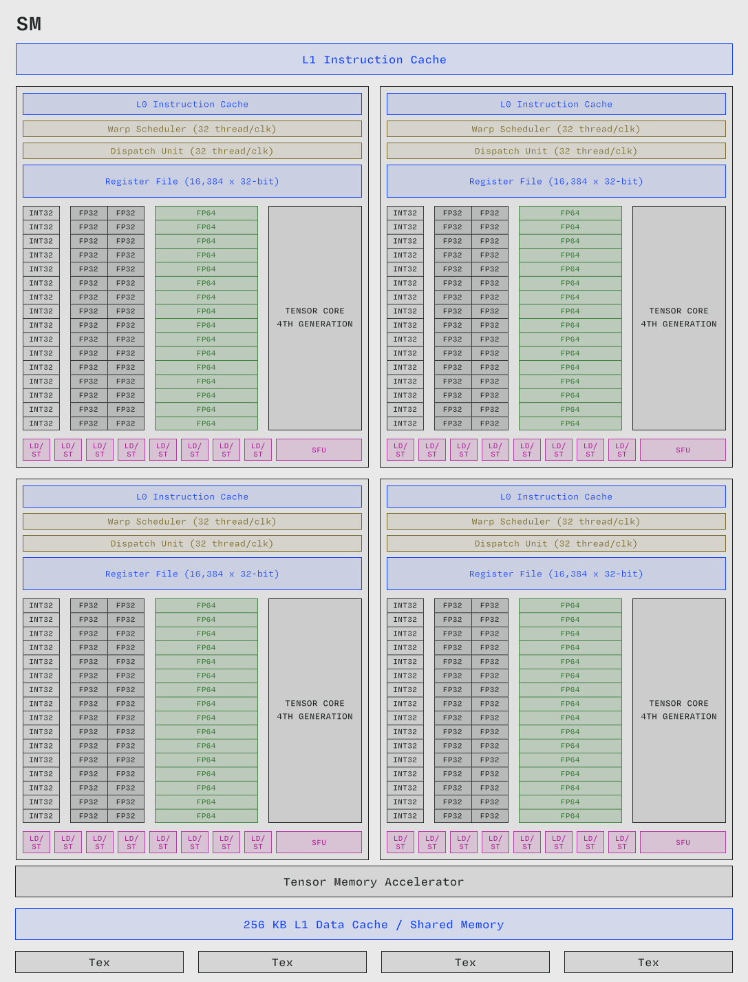
H100 流式多处理器(SM)的内部架构图。浅蓝色部分描绘的是 L1 数据缓存。修改自 NVIDIA 的 H100 白皮书。
每个 SM 会将该内存分配给调度到其上的 线程块。
L1 数据缓存与执行计算的组件(例如 CUDA 核心)位于同一位置,其速度仅比这些组件慢约一个数量级。
它采用 SRAM 实现,这种基础半导体单元也用于 CPU 缓存、寄存器以及 Groq LPU 内存子系统。L1 数据缓存由 SM 的 加载/存储单元 访问。
CPU 同样设有 L1 缓存,但是在 CPU 中,该缓存完全由硬件管理。而在 GPU 中,该缓存主要由程序员管理,即使在使用高级语言(如 CUDA C)时也是如此。
H100 的每个 SM 中的 L1 数据缓存可存储 256 KiB(2,097,152 位)。在 H100 SXM 5 的 132 个 SM 中,总计提供 33 MiB(242,221,056 位)的缓存空间。
英文原文(Modal GPU Glossary)
The L1 data cache is the private memory of the Streaming Multiprocessor (SM).
.](themed-image://gh100-sm.svg)
Each SM partitions that memory among groups of threads scheduled onto it.
The L1 data cache is co-located with and only about an order of magnitude slower than the components that effect computations (e.g. the CUDA Cores).
It is implemented with SRAM, the same basic semiconductor cell used in CPU caches and registers and in the memory subsystem of Groq LPUs. The L1 data cache is accessed by the Load/Store Units of the SM.
CPUs also maintain an L1 cache. In CPUs, that cache is fully hardware-managed. In GPUs that cache is mostly programmer-managed, even in high-level languages like CUDA C.
Each L1 data cache in each of an H100's SMs can store 256 KiB (2,097,152 bits). Across the 132 SMs in an H100 SXM 5, that's 33 MiB (242,221,056 bits) of cache space.
相关词条
本词条改编自 Modal GPU Glossary(CC BY 4.0)· 中文翻译 miter6/gpu-glossary-zh,MAE 整理排版。